Introducing MOSFET
The metal-oxide-semiconductor field-effect transistor (MOSFET) has become the most commonly used transistor in integrated circuits and electronic devices. MOSFETs have almost completely replaced bipolar junction transistors (BJTs) in digital circuits due to several advantageous characteristics. We will explore the working principles, structure, types, and applications of MOSFETs at an introductory level.
MOSFET Structure and Composition
A MOSFET is a special type of field-effect transistor where a gate electrode is placed over a semiconductor substrate that has an undetectable layer of insulating material like silicon dioxide. This forms a metal-insulator-semiconductor layered structure that gives rise to the name “metal-oxide-semiconductor.” The four terminals of a MOSFET device are called source (S), gate (G), drain (D), and body/substrate (B). The semiconductor substrate on which the layers are fabricated is typically high-purity silicon, doped appropriately, to form n-channel or p-channel MOSFETs. Impurity atoms like phosphorus or boron are precisely introduced in a process called doping to alter the number of free charge carriers.

Fig 1: Basic Construction of MOSFET
Operating Principle of MOSFET
The MOSFET is a transistor designed to be used as a voltage-controlled switching device. The core functionality of this integrated circuit relies on forming an inversion channel that conducts current between the source and drain terminals in the underlying layer of semiconductor material. The formation of this conducting channel is controlled by an electrically isolated gate electrode, which sits on top of a thin insulating dielectric oxide layer residing over the substrate. By applying a voltage to this gate, an electric field develops across the insulating dielectric layer, which in turn influences the concentration and flow of carriers within the silicon underneath.
Specifically, in an n-channel, enhancement-mode type of MOSFET, applying a positive gate voltage that surpasses a defined threshold voltage causes electrons to be drawn toward the oxide-semiconductor interface. Here they accumulate to form an n-type, electron-rich region known as an inversion layer or n-channel. The source and drain terminals have n-type semiconductor deposits on opposite sides of the created channel.
Therefore, when the n-channel is induced, it allows current flow between the electron-rich n-type source and drain regions, turning the device ON like a closed switch. The gate itself draws negligible control current, while the channel modulation occurs between the drain and the source. Removing the gate voltage causes the inversion layer to disappear and switches the device into a non-conducting OFF state with very small current. This voltage-activated formation of the inversion channel makes the MOSFET behave as an electrically operated switch. The gate voltage amplitude controls whether the switch is ON, allowing full conduction between sources and drain terminals or switched OFF.
Types of MOSFET
The following are the main categories of MOSFET and a brief description of their work.
-
Enhancement-type MOSFET
The enhancement type MOSFET (E-MOSFET) operates solely in enhancement mode, as shown in Figure 4(b), without any depletion mode capabilities. Unlike the depletion type MOSFET, the E-MOSFET does not have a built-in channel for electric current to flow between the drain and source terminals. Instead, the E-MOSFET requires a positive voltage applied to the gate terminal above a minimum threshold voltage to induce a conducting channel in the substrate region next to the insulating oxide layer separating the gate. Applying a gate voltage above this threshold causes an inversion layer in the p-type semiconductor substrate, allowing electron carriers to flow and create a current channel.
Increasing the positive gate voltage further pulls more free electrons into this induced channel, increasing the conductivity through the E-MOSFET. When the gate voltage falls back below the threshold, the induced channel disappears, preventing any current flow through the transistor. Schematic symbols used for n-channel or p-channel E-MOSFETs contain broken lines for the channel, indicating no permanent physical channel. An inward arrow on the gate represents an n-channel E-MOSFET using electron carriers, while an outward arrow represents a p-channel version using hole carriers. Some E-MOSFET designs also provide a separate electrical connection to the transistor substrate.
-
N-channel MOSFET
This MOSFET has electrons as the majority carrier for conduction from an n-type source to an n-type drain. Fig 2 shows its symbol.

Fig 2: Enhancement Type N-Channel
-
P-channel MOSFET
Such MOSFET has holes as the majority carrier for conduction from a p-type source to a p-type drain. The schematic symbol is shown in Fig 3.
Fig 3: Enhancement Type P-Channel

Fig 4: Operation of D-MOSFET and E-MOSFET
-
Depletion MOSFET
The depletion MOSFET (D-MOSFET) is another type of MOSFET. It contains drain and source regions, which have diffused into either side of a narrow semiconductor channel region adjacent to the insulated gate electrode. This gate, channel, drain, and source structure is entirely embedded within a p-type or n-type substrate material.
Both n-channel and p-channel configurations exist for the D-MOSFET with the same overall functionality but requiring opposite voltage polarities during operation. Applying a negative gate-source voltage to an n-channel D-MOSFET places it into depletion mode operation. This is because the negative gate voltage creates an electric field that repels mobile electrons away from the n-type channel. With fewer free electrons, the channel takes on a more positive charge as it becomes depleted of carriers.
This depletion of mobile electrons reduces the channel’s conductivity. Suppose the negative gate voltage keeps increasing in magnitude. In that case, more conduction electrons get repelled from the channel until voltage VGS (off) is reached, at which point the channel is fully depleted of carriers. Past this voltage, the drain current flow stops. This depletion-mode behavior is analogous to an n-channel JFET, allowing drain current for negative VGS voltages down to the pinch-off voltage VGS (off). For positively applied VGS voltages, the n-channel D- MOSFET enters enhancement mode operation like a traditional E-MOSFET by accumulating excess electrons within an induced inversion channel. Hence, the D-MOSFET conducts current for both negative and positive gate voltages.
-
D-MOSFET Symbols
The D-MOSFET schematic symbols shown below connect the substrate (indicated by an arrow) internally to the source. In some cases, a separate substrate pin exists. The substrate determines the polarity for the drain and source diffusions.
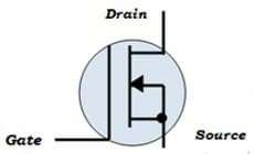
Fig 5: Depletion Type N-Channel
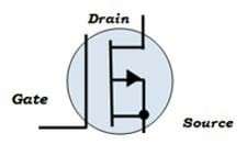
Fig 6: Depletion Type P-Channel
Applications of MOSFETs
Due to their compact size, low cost, and advanced fabrication techniques, MOSFETs have found extremely widespread use in:
-
Digital Logic Circuits
CMOS (Complementary MOS) logic uses paired integrated n-channel and p-channel MOSFETs to implement complex logic functions and gates with high noise immunity. Microprocessors, DRAM, sensors, and other electronic devices use CMOS due to its low static power consumption. NMOS logic using only n-channel MOSFETs is also popular in digital circuits.
-
Analog Circuits
MOSFETs play an essential role in amplifying analog signals linearly, and designers use them extensively in analog integrated circuits. They find application in a wide range of circuits, including analog amplifiers, active filters, oscillators, RF mixers, phase-locked loops, voltage-controlled oscillators, and more. MOSFET parameters like transconductance allow tuning analog performance.
-
Power Electronics
Power MOSFETs are capable of controlling high voltages up to 1000V and currents up to 100A. Uses include switched-mode power supplies, DC-AC inverters for motor control, uninterruptible power supplies, automotive electronics, actuators, and other industrial applications. Power MOSFETs provide low resistive losses and fast switching capabilities.
-
Memories and Microprocessors
ICs have enabled extremely dense and compact non-volatile memories such as EEPROM and Flash memory by integrating ultra-large-scale MOSFETs. Firmware, data storage, and other purposes utilize these memories. Microprocessors integrate tens of millions of MOSFETs to implement arithmetic logic units, control units, caches, and other subsystems, providing enormous computing power.
-
Sensors
Miniaturized and low-power MOSFETs built using advanced fabrication can sense physical, chemical, and biological signals. Application areas include gas sensors, biosensors, MEMS, environmental monitoring, and more. CMOS fabrication allows the integration of sensing and processing functions.
Conclusion: Understanding MOSFET Power
In summary, the metal-oxide-semiconductor field-effect transistor (MOSFET) reigns supreme in modern electronics, supplanting bipolar junction transistors (BJTs). Our exploration covered MOSFET structure, working principles, and types, showcasing their versatility in digital and analog circuits, power electronics, memories, microprocessors, and sensors. As a testament to innovation, MOSFETs offer compactness, cost-effectiveness, and efficiency, shaping the landscape of contemporary electronics. This journey lays the foundation for a profound understanding of MOSFETs and their pivotal role in electronic evolution.

Fatima Razzaq is a freelance technical writer who served as an electrical engineering lecturer at Air University—a federally chartered public sector research university in Pakistan. Razzaq holds a Bachelor’s degree with distinction in electronic engineering from Ghulam Ishaq Khan Institute of Engineering Sciences and Technology (GIKI) and a Master’s degree in Sustainable Transportation and Electrical Power Systems from the University of Nottingham, Universidad de Oviedo, and La Sapienza University of Rome. Razzaq’s diverse work experiences in academia and industry continue to inform her prolific technical writing journey in the areas of electrical engineering, storage mechanisms, power electronics, electric vehicles, energy, and related topics.