The Fundamental Role of Transistors in Modern Electronics
Transistors are electronic devices that are building blocks of ICs, both analog and digital. These are among the most commonly used electronic components. That’s why almost all novel technologies use transistors in one way or another. These technologies range from bullet trains to remote control. Transistors have three terminals, and they are doped semiconductor devices. Transistors perform two main functions: switching and amplification.
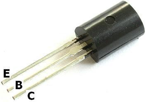
Figure 1: Transistor
There are two major families of transistors: FETs and BJTs. The transistors can be either bipolar or unipolar. The charge carriers for bipolar transistors are electrons and holes. BJTs are examples of bipolar transistors. The charge carriers for unipolar transistors can be either electrons (in the case of n-channel) or holes (in the case of p-channel). MOSFETs and JFETs are examples of unipolar transistors.
The two major configurations for transistors are PNP and NPN. The PNP refers to positive–negative–positive. It has two layers of positive semiconductors and one layer of negative semiconductors. The NPN refers to negative-positive-negative. It has two layers of negative semiconductors and one layer of positive semiconductors.
Terminals and Doping Characteristics of a Transistor
There are three terminals within a transistor, as Figure 1 indicates. The base(B), the emitter(E), and the collector(C). Normally, the base is lightly doped and has a small width. The emitter is heavily doped and is of normal width. The collector is moderately doped and is larger in width than both the base and the emitter. These are shown in the figure 2.

Figure 2: Terminals within transistor
Working of NPN Transistor
NPN Transistor Configuration
In an NPN transistor, the collector and the emitter are doped with an n-type impurity, whereas the base is doped with a p-type impurity. This is shown in the figure below:

Figure 3: NPN Transistor Configuration
The positive voltage is applied to the collector, and the direction of conventional current is from the collector to the emitter. The majority of charge carriers in n-type regions, i.e., emitter and collector, are electrons, and minority charge carriers are holes. The majority charge carriers in p-type regions, i.e., base are holes, and electrons are minority charge carriers. Hence, the majority of charge carriers in an NPN transistor are electrons.
NPN Transistor Symbol
The symbol for an NPN transistor is shown below:

Figure 4: Symbol for an NPN Transistor
Circuit Diagram for NPN Transistor
In the NPN transistor, two pn junctions are formed; one is the emitter-base junction, and the other is a collector-base junction. The transistor works in active mode, so the base-emitter junction is forward-biased, and the collector-base junction is reverse-biased through supply voltage. The collector and the emitter are connected with the battery terminals as shown below:

Figure 5: NPN Transistor Circuit Diagram
The majority of charge carriers in the emitter, i.e., electrons, flow towards the base, which is p-type and is positive. The flow of electrons is known as current, so the flow of electrons from emitter to base is referred to as emitter current or IE.
The base has less number of holes as it is lightly doped and is narrow as compared to the emitter and collector. Consequently, few electrons will combine with the holes, and the majority of electrons will pass through the base. This resultant flow of electrons is called base current IB, and it is very small.
The positive terminal of the battery will attract the remaining electrons. Consequently, the electrons will start flowing across the collector-base junction. This is known as collector current IC.
The relation between base current Ib, collector current IC, and emitter current IE is given by the following equation:
IE = IB + IC
In DC mode, the relation between IE and IC can be expressed in terms of DC gain as follows:
IC = IE
For ideal cases, the value is equal to one. However, in practical cases, the value is between 0.90 to 0.998.
In DC mode, the relation between IE and IC can be expressed in terms of DC gain as follows:
Working of PNP Transistor:
PNP Transistor Configuration
In a PNP transistor, the collector and the emitter are doped with p-type impurity, whereas the base is doped with n-type impurity. This is shown in the figure below:

Figure 6: PNP Transistor Configuration
PNP Transistor Symbol
The negative voltage is applied on the collector, and the direction of conventional current is from emitter to collector. The majority of charge carriers in p-type regions, i.e., emitter and collector, are holes, and minority charge carriers are electrons. The majority charge carriers in n-type regions, i.e., bases are electrons, and holes are minority charge carriers. Hence, the majority of charge carriers in a PNP transistor are holes. The symbol for the PNP transistor is shown below:

Figure 7: Symbol for PNP transistor
Circuit Diagram for PNP Transistor
In the PNP transistor, two pn junctions are formed; one is the emitter-base junction, and the other is a collector-base junction. The transistor works in active mode, so the base-emitter junction is connected in a forward-biased configuration, and the collector-base junction is connected in a reverse-biased configuration through supply voltage. The collector and the emitter are connected with the battery terminals as shown below:

Figure 8: PNP Transistor Circuit Diagram
When the positive voltage is applied to the emitter, the majority of charge carriers in the emitter, i.e., holes, flow towards the base, which is n-type and negative. The holes are attracted to electrons and flow towards the base. This flow of holes from emitter to base is referred to as emitter current or IE.
The base has fewer electrons as it is lightly doped and narrower than the emitter and collector. Consequently, few holes will combine with the electrons, and the majority of holes will pass through the base. This resultant flow of holes is called base current IB, and it is very small.
The negative terminal of the battery will attract the holes. Consequently, the holes will start flowing across the collector-base junction. This is known as collector current IC.
The relation between base current Ib, collector current IC, and emitter current IE is given by the following equation:
IE = IB + IC
The following equation gives the collector current:
IC = IE – IB
The base current is generally 2% of the emitter current, and the collector current is 98% of the emitter current.
Differences Between PNP and NPN Transistors:
The major differences between PNP and NPN transistors are as follows:
- The major difference between PNP and NPN transistors is the doping of the emitter, base, and collector. In the PNP transistor, the emitter and collector are doped with a p-type dopant, and the base is doped with an n-type impurity or dopant. In the NPN transistor, the emitter and collector are doped with n-type impurities, and the base is doped with p-type impurities. The PNP and NPN transistor can be interpreted as positive-negative-positive for PNP and negative-positive-negative for NPN configuration.
- The majority of charge carriers in the NPN transistor are electrons, whereas the majority of charge carriers in the PNP transistor are holes. The minority charge carriers in the PNP transistor are electrons, whereas the minority charge carriers in the NPN transistor are holes. Due to swift electron movement as compared to the hole, current conduction in the NPN transistor is relatively high as compared to the PNP transistor.
- The direction of flow of current for a PNP transistor is from emitter to collector. However, the direction of flow of current for an NPN transistor is from collector to emitter. Consequently, the symbols of the PNP and NPN transistors are different from each other.
- The PNP transistor ‘turns on’ when the holes enter the base region, whereas the NPN transistor ‘turns on’ when the electrons enter the base region. In the PNP transistor, a small current flows through the base and enters the emitter junction, whereas in the NPN transistor, a small current flows through the emitter and enters the base junction.
- The switching is low for the PNP transistor and high for the NPN transistor. The ground signal is high for the PNP transistor and low for the NPN transistor.
Applications of PNP and NPN Transistors in the Modern World:
ICs comprising transistors are the building blocks of all modern gadgets, making their uses wide-ranging. Mentioned below are some important applications.
- They are used in TVs, radios, and other telecommunication devices for frequency amplification and regulation.
- The PNP and NPN transistors are also used in computers and are core components within the circuitry.
- Transistors are also used in power generation devices. Nowadays, transistors are used in inverter circuitry within renewable energy systems, such as solar systems, to convert DC power into AC power.
- The PNP and NPN transistors are also used in biomedical monitoring and measuring equipment, ECG amplifiers, EMG amplifiers, EEG amplifiers, pacemakers, neurostimulators, etc.
- The PNP and npn transistors are also used in sensor and control systems, Electronic Stability Control (ESC), Transmission Control Systems (TCUs), Anti-lock Braking systems (ABS), Electronic Power Steering (EPS), and Engine Control Units (ECUs) of an automobile to ensure smooth function and performance.

Fatima Razzaq is a freelance technical writer who served as an electrical engineering lecturer at Air University—a federally chartered public sector research university in Pakistan. Razzaq holds a Bachelor’s degree with distinction in electronic engineering from Ghulam Ishaq Khan Institute of Engineering Sciences and Technology (GIKI) and a Master’s degree in Sustainable Transportation and Electrical Power Systems from the University of Nottingham, Universidad de Oviedo, and La Sapienza University of Rome. Razzaq’s diverse work experiences in academia and industry continue to inform her prolific technical writing journey in the areas of electrical engineering, storage mechanisms, power electronics, electric vehicles, energy, and related topics.